
Research Overview

Our research focuses on the optical and electronic properties of emerging semiconductor such as perovskites, to control the absorption or emission of light and/or manipulate the transport and recombination of energised charge carriers in these materials. We employ a number of cutting edge characterization techniques (ultrafast lasers, synchrotron x-ray) to study the photophysics of materials and devices with high spatial and temporal resolutions. Our work finds a number of applications including light harvesting (photovoltaics, photo- and X-Ray- detectors) and light emission (LEDs, lasers) devices.
Materials Synthesis and Charcterization

We develop and synthesise new semiconductor materials, and characterise them using a modern toolbox of materials chemistry: X-Ray and electron diffraction, solid-state NMR, electron microscopy and optical spectroscopies. A particularly unique aspect is the development of multimodal techniques to interrelate a series of different measurements to provide connections between the materials, chemical, physical, optical, morphological and structural properties – where possible on the same local scan area. Recent work has focused on pushing new nano-structured emitters further into the blue spectral region, and molecular modulation/passivation protocols for different bandgap bulk halide perovskites to increase their performance and long-term device stability.
Spectroscopy
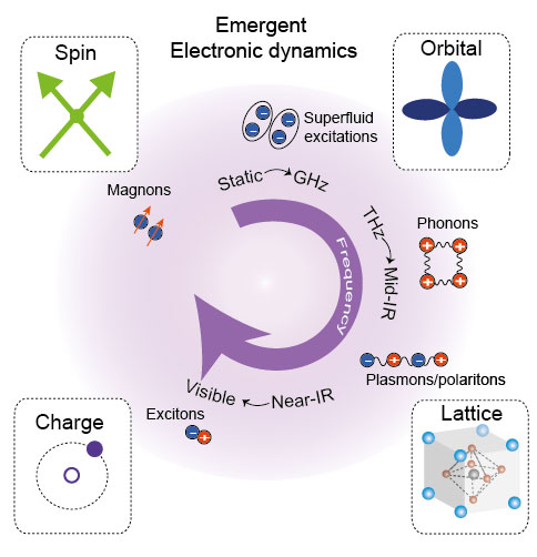
A precise understanding of the physical principles governing the structural and electronic dynamics in electronic materials is necessary to generate insights that are subsequently fed to the development of next generation energy efficient devices. We investigate the interaction of light with matter, using light absorption or photoluminescence (PL) techniques to access key information about optoelectronic properties in materials and devices. To better inform synthetic efforts, and understand the critical roles of heterogeneity, interfaces, and disorder, we investigate the materials using various excitation sources such as ultrafast lasers. We perform a number of techniques including time-resolved photoluminescence and transient absorption across a range of time scales relevant to carrier recombination and device operation.
Optoelectronic Devices
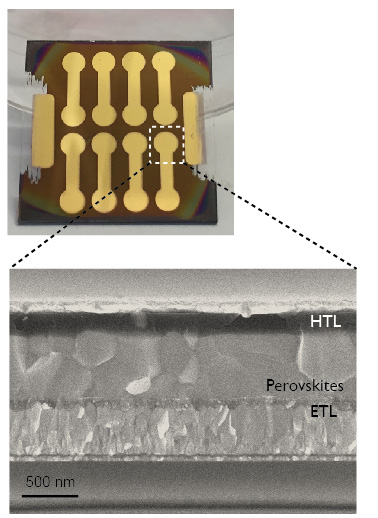
Materials with highly crystalline lattice structures and low defect concentrations have classically been considered essential for high-performance optoelectronic devices. However, the emergence of high-efficiency devices based on emerging hybrid semiconductors is provoking researchers to rethink this traditional picture, as the heterogeneity in several properties within these materials occurs on a series of length scales. In materials typically fabricated crudely through simple processing techniques, there are large local fluctuations in defect density and lattice structure that appear from short to long length scales (<100 nm to >10 µm). We covers a range of inexpensive devices which convert incident photons into other forms of energy. This includes efficient photovoltaics, as well as photo-detectors.
